Product Summary
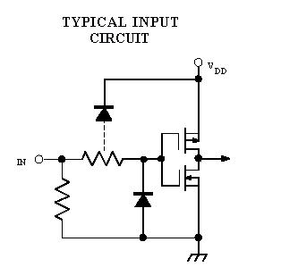
Designed primarily for use with high-voltage vacuum-fluorescent displays, the UCN5815A BiMOS II integrated circuit consists of eight npn Darlington source drivers with output pull-down resistors, a CMOS latch for each driver, and common STROBE,BLANKING, and ENABLE functions. The bipolar outputs may be used as segment, dot (matrix), bar, ordigit drivers in vacuum-fluorescent displays. All eight outputs can beactivated simultaneously at ambient temperatures in excess of 75℃. To simplify printed wiring board layout, output connections areopposite the inputs.
Parametrics
UCN5815A absolute maximum ratings: (1)Output Voltage: 60 V; (2)Logic Supply Voltage Range:4.5 V to 15 V; (3)Load Supply Voltage Range: 5.0 V to 60 V; (4)Input Voltage Range: -0.3 V to VDD + 0.3 V; (5)Continuous Output Current: -40 mA; (6)Package Power Dissipation: 2.5 W; (7)Operating Temperature Range: -20℃ to +85℃; (8)Storage Temperature Range: -55℃ to +150℃; (9)Derate linearly to 0 W at +150℃.
Features
UCN5815A features: (1)To 4.4 MHz Date-lnput Rate; (2)High-Voltage Source Outputs; (3)CMOS, NMOS, TTL Compatible Inputs; (4)Low-Power CMOS Latches; (5)Internal Pull-Down Resistors; (6)Wide Supply-Voltage Range.
Diagrams

| Image | Part No | Mfg | Description |  |
Pricing (USD) |
Quantity | ||||
|---|---|---|---|---|---|---|---|---|---|---|
 |
 UCN5815A |
 Other |
 |
 Data Sheet |
 Negotiable |
|
||||
| Image | Part No | Mfg | Description |  |
Pricing (USD) |
Quantity | ||||
 |
 UCN5800A |
 Other |
 |
 Data Sheet |
 Negotiable |
|
||||
 |
 UCN5804B |
 Other |
 |
 Data Sheet |
 Negotiable |
|
||||
 |
 UCN5810A |
 Other |
 |
 Data Sheet |
 Negotiable |
|
||||
 |
 UCN5810AF |
 Other |
 |
 Data Sheet |
 Negotiable |
|
||||
 |
 UCN5810EPF |
 Other |
 |
 Data Sheet |
 Negotiable |
|
||||
 |
 UCN5810LWF |
 Other |
 |
 Data Sheet |
 Negotiable |
|
||||
 (China (Mainland))


